Investigating the Influence of Doping on the Physical and Optical Behavior of Nanomaterials
Madhavi Sharad Darekar*, Praveen Beekanahalli Mokshanatha
Department of Chemistry, Institute of Engineering and Technology, Srinivas University, Mukka, Surathkal, Mangalore - 574146, Karnataka, India
*Corresponding author 2: Madhavi Sharad Darekar, Department of Chemistry, Institute of Engineering and Technology, Srinivas University, Mukka, Surathkal, Mangalore - 574146, Karnataka, India
Received: 16 June 2025; Accepted: 26 June 2025; Published: 20 August 2025
Article Information
Citation: Madhavi Sharad Darekar, Praveen Beekanahalli Mokshanatha. Investigating the Influence of Doping on the Physical and Optical Behavior of Nanomaterials. Journal of Nanotechnology Research. 7 (2025): 13-26.
DOI: 10.26502/jnr.2688-85210048
View / Download Pdf Share at FacebookAbstract
The study involved the synthesis of Thioglycerol-capped undoped cadmium sulphide (CdS) and copper sulphide (Cu2S) nanoparticles, and Mn-doped diluted magnetic semiconductor (DMS) CdS and Cu2S nanoparticles using a room-temperature, non-aqueous chemical method. Undoped CdS and Cu2S thin films, Mn-doped CdS, and Cu2S thin films were fabricated on fluorine-doped tin oxide (FTO) glass substrates via dip coating, followed by annealing at 420°C in air for 20 minutes. The optical properties of CdS, Cu2S, CdS:Mn, and Cu2S:Mn nanoparticles were investigated using Ultraviolet-Visible (UV-Vis) absorption and photoluminescence (PL) spectroscopy. Energy Dispersive X-ray Analysis (EDAX) was employed to determine the chemical composition of undoped CdS and Cu2S and Mn-doped CdS and Cu2S thin films and the FTO glass substrates, with chemical composition percentages determined using mapping techniques. This study highlights the contrasting experimental outcomes of undoped and doped nanoparticles and thin films, emphasizing the advantages of doped materials in various applications over their undoped counterparts. Specifically, it aims to demonstrate the enhanced performance and suitability of doped materials in diverse settings.
Keywords
Synthesis; Characterization; Non-aqueous chemical method; Nanoparticles; Thin films; Dip coating method
Synthesis articles; Characterization articles; Non-aqueous chemical method articles; Nanoparticles articles; Thin films articles; Dip coating method articles
Article Details
Introduction
CdS is a yellow, direct band gap semiconductor with a band gap of approximately 2.42 eV. CdS semiconductor has optoelectronic applications like solar cells (often used as a window layer or in heterojunctions with other materials), photodetectors, light-emitting diodes (LEDs), thermoelectric devices, display devices etc. and it is used as a pigment due to its good thermal stability, light and weather fastness, chemical resistance, and high opacity. CdS is an II-VI group n-type semiconductor, meaning it has an excess of electrons. CdS exists in two polymorphs: a more stable hexagonal wurtzite structure (greenockite) and a cubic zinc blende structure (hawleyite). CdS is highly photosensitive in the visible region, meaning its conductivity increases when exposed to light. It has a high mobility, a high absorption coefficient, a high refractive index, and high electrochemical stability. CdS is used in thin-film solar cells, often as a window layer. Its photosensitivity makes it suitable for use in photodetectors. CdS is used in photoconductive sensors. CdS finds applications in photonic devices. CdS was one of the first semiconductor materials used in thin-film transistors (TFTs). CdS luminesces under electron beam excitation and is used as a phosphor. CdS is used in photocatalysis, where it can be used to degrade organic dyes. CdS nanocomposites can be used for hydrogen production via water splitting. CdS can be used in core/shell CdSe/CdS quantum dots [1-7]. Cu2S is a I-VI group p-type semiconductor with an indirect band gap of 1.21 eV, making it a promising material for solar energy conversion, nanoscale sensors, and cathodes in lithium-ion batteries. Cu2S is a good material for solar energy absorbers due to its non-toxic, low-cost nature, and suitable band gap. It is used as the absorber of visible light. It is suitable for potential applications in solar cells (often used as an absorber layer or in heterojunctions with other materials), photodetectors, thermoelectric devices, display devices, photocatalyst, biosensors, gas sensors, field emission devices, and nano switches. Cu2S can form in cubic or tetragonal structures depending on the preparation method. Various methods can be used to synthesize Cu2S nanostructures, including nanolithography, template-directed synthesis, vapour-phase methods, and solvothermal methods. The advantages of Cu2S semiconductor material are: i) High elemental earth abundance:- Cu and S are readily available, ii) Nontoxicity:- Cu2S is a non-toxic material, iii) Suitable optical properties:- Cu2S has a high absorption coefficient of over 104 cm-1 iv) Low cost, and v) Ideal band gap for solar energy absorption [1, 3, 8-15].
Undoped CdS and Cu2S nanoparticles can be synthesized via various chemical and physical methods, including sol-gel, chemical bath deposition, microwave-assisted synthesis, and hydrothermal, among others [14]. The chemical methods like sol-gel method, chemical bath deposition, aqueous precipitation, microwave-assisted synthesis, and solvothermal method were used for the synthesis of undoped CdS nanoparticles. The sol-gel method involves using precursors like cadmium acetate and thioacetamide to form a sol and then a gel, which can then be processed to obtain CdS nanoparticles. The chemical bath deposition technique involves reacting cadmium and sulfur precursors in a solution, resulting in the precipitation of CdS nanoparticles. The aqueous precipitation method utilizes cadmium nitrate and sodium sulfide precursors to produce a yellow CdS precipitate. The microwave-assisted synthesis method uses microwave irradiation to facilitate the reaction of precursors in aqueous solutions, leading to the formation of CdS nanoparticles. The solvothermal method involves reacting precursors in a closed vessel under high temperature and pressure to control the morphology and size of the CdS nanoparticles. The physical methods like laser ablation, and hydrothermal method were used to synthesize the undoped CdS nanoparticles. The hydrothermal method involves reacting precursors in a sealed vessel under high temperature and pressure, which can control the morphology and size of the CdS nanoparticles. The laser ablation method uses laser energy to ablate a target material (e.g, CdS) and deposit the resulting nanoparticles onto a substrate. The other methods like template-based method, micelles, sonochemical and arrested precipitation in homogeneous solution were also used for the synthesis of undoped CdS nanoparticles [1-3, 15-20]. The undoped Cu2S nanoparticles were synthesized using the chemical methods like wet chemical method, and microwave-assisted synthesis. The wet chemical method involves reacting copper and sulfur precursors in solution, leading to the formation of Cu2S nanoparticles. Similar to CdS, the microwave-assisted synthesis method can be used for Cu2S synthesis, with precursors like copper acetate and sodium sulfide. The undoped Cu2S nanoparticles were also synthesized using the physical methods like thermal treatment, electrochemical synthesis and deposition and sputtering techniques. Decomposition of Cu precursors at high temperatures (calcination or pyrolysis) can also be used to generate Cu2S nanoparticles. The electrochemical synthesis method involves controlling the rate of reduction of Cu species to produce Cu and Cu2S nanoparticles. The deposition and sputtering techniques provide more size-selective synthesis of Cu and Cu-based nanoparticles [1, 2, 8, 23]. Undoped CdS and Cu2S thin films can be prepared using the dip coating method, a simple and cost-effective technique that involves immersing a substrate into a solution and withdrawing it at a controlled rate. The dip coating method involves immersing a substrate into a solution containing the precursor materials (e.g, cadmium chloride and thiourea for CdS, copper acetate and thiourea for Cu2S) and then withdrawing it at a controlled rate. The solution is typically dissolved in a solvent like methanol. The deposited thin films are then typically heat-treated (annealed) in air to improve their structural and optical properties. Dip coating is a relatively simple and inexpensive method compared to other thin-film deposition techniques. It is suitable for depositing thin films on large area substrates. The process is relatively easy to control and reproduce. CdS is a semiconductor material with a wide range of applications, including solar cells and optoelectronic devices. Cu2S is another semiconductor material that can be used in solar cells and other applications. The properties of the prepared thin films are typically characterized using techniques like XRD, SEM, and UV-Vis absorption spectroscopy. CdS and Cu2S thin films are used as absorber layers in thin-film solar cells. They can also be used in other optoelectronic devices, such as photodetectors and light-emitting diodes [1-3, 8, 24, 25]. Mn-doped CdS and Cu2S nanoparticles are semiconductor nanoparticles with potential applications in various fields, including photocatalysis and luminescence, with Mn doping enhancing their properties. Mn-doped CdS nanoparticles can be synthesized via methods like co-precipitation, chemical precipitation, and green capping with starch. XRD studies reveal a cubic phase structure for CdS nanoparticles, with Mn doping potentially influencing the morphology and size. Mn doping modifies the luminescent, optical, and electronic properties of CdS, potentially leading to a decrease in band gap energy. Mn-doped CdS exhibits interesting luminescent properties, with the luminescence intensity being influenced by Mn concentration and synthesis conditions. Mn doping can enhance the photoconductivity of CdS, making it suitable for applications in optoelectronic devices. Mn doping can change the morphology of CdS nanoparticles from spherical to scale-like structures. The dielectric properties and AC conductivity of CdS are affected by Mn doping, which can be investigated over a wide frequency range and temperature range. Mn doping can also modify the ferromagnetic properties of CdS. Mn-doped CdS nanoparticles are used in photocatalytic applications, such as hydrogen production and dye degradation. They are used in luminescent materials for applications in displays, sensors, and bioimaging [26-34]. Mn-doped Cu2S nanoparticles can be synthesized using wet chemical routes. XRD studies reveal a hexagonal crystal structure for Cu2S nanoparticles. Cu2S nanoparticles exhibit optical properties that can be tuned by controlling their size and morphology. Cu2S nanoparticles can be used in photocatalytic applications, such as hydrogen production and dye degradation. Cu2S nanoparticles have potential applications in energy storage devices [35-37].
Mn-doped CdS and Cu2S thin films prepared by the dip coating method exhibit potential for optoelectronic applications, with studies exploring their structural, optical, and electrical properties, and the effects of Mn doping on CdS. Mn-doped CdS thin films can be prepared using the dip coating method, where the substrate is immersed in a solution containing cadmium and sulphur precursors, along with Mn dopant. Mn doping can modify the structural, optical, and electrical properties of CdS films. These films are explored for applications in optoelectronic devices, solar cells, and other areas. Techniques like XRD, SEM, and UV-Vis absorption spectroscopy are used to characterize the films. Mn-doped Cu2S thin films can also be prepared using the dip coating method, involving immersion of the substrate in a solution containing copper and sulphur precursors. Cu2S films are explored for applications in solar cells and other optoelectronic devices. Similar to CdS, characterization techniques like XRD, SEM, and UV-Vis absorption spectroscopy are used to study the films [1-3, 8, 35, 38-40]. Several methods can be used to prepare CdS and Cu2S thin films and also Mn-doped CdS and Cu2S thin films, including dip coating, spray pyrolysis, spin coating, chemical bath deposition, and successive ionic layer adsorption and reaction (SILAR). While dip coating offers advantages like simplicity, low cost, and ease of film thickness control, other methods like spray pyrolysis, spin coating, SILAR, and chemical bath deposition may be preferred for specific applications. Dip coating is a relatively simple and cost-effective method, requiring less specialized equipment than other techniques. Film thickness can be easily controlled by adjusting parameters like dip time, concentration, and draw speed. Dip coating can be adapted to produce films with specific nanostructures, such as nanoparticles or nanorod arrays, by using appropriate precursor solutions. The best method for preparing CdS and Cu2S thin films and also Mn-doped CdS and Cu2S thin films depends on the specific application requirements, such as film thickness, uniformity, composition, and desired nanostructures. Dip coating offers simplicity and cost-effectiveness, while other methods like spray pyrolysis, spin coating, CBD, and SILAR may be more suitable for specific applications [1-3, 8, 35, 41-45]. In the present paper, the undoped and Mn-doped CdS and Cu2S nanoparticles were synthesized using the wet chemical method at room temperature. These nanoparticles were characterized by UV-Vis absorption spectroscopy and PL spectroscopy. Then the undoped and Mn-doped CdS and Cu2S thin films were deposited on FTO glass slides by the dip coating method. The thin films, after being heat-treated in air at 420°C for 20 minutes, were analyzed using EDAX to determine their elemental composition. This study contrasts the experimental and characterization outcomes of undoped and Mn-doped CdS and Cu2S nanoparticles and thin films, highlighting the advantages of Mn doping in these materials. Specifically, it demonstrates how Mn doping alters the properties of both the nanoparticles and thin films, showcasing potential improvements in performance.
Experimental
Thioglycerol capped undoped and Mn-doped CdS and Cu2S nanoparticles were prepared by the wet chemical synthesis at room temperature in our previous study [1, 2, 8, 26, 35]. These nanoparticles were analyzed by UV-Vis absorption spectroscopy and PL spectroscopy. The Analytical Reagent (A.R.) grade chemicals like cadmium acetate, thioglycerol and sodium sulphide were used for the synthesis of undoped CdS nanoparticles and the chemicals like cadmium acetate, manganese chloride, thioglycerol and sodium sulphide were used for the synthesis of Mn-doped CdS nanoparticles. Ethanol was used as the solvent in the synthesis of undoped and Mn-doped CdS nanoparticles. The undoped CdS nanoparticles were synthesized by varying the thioglycerol concentration and by keeping the molarities of cadmium acetate and sodium sulphide constant. The Mn-doped CdS nanoparticles were synthesized by changing the concentration of manganese chloride and by keeping the molarities of cadmium acetate, thioglycerol and sodium sulphide constant. Similar to CdS, the undoped Cu2S nanoparticles were prepared by varying the thioglycerol concentration and by keeping the molarities of cuprous chloride and sodium sulphide constant. The Mn-doped Cu2S nanoparticles were synthesized by changing the concentration of manganese chloride and by keeping the molarities of cuprous chloride, thioglycerol and sodium sulphide constant [1, 2, 8, 26, 35]. A CdS thin film approximately 280 nm in thickness was prepared on the FTO glass slide by the dip coating method with 2300 dip times. Similarly, a Cu2S thin film approximately 26 μm in thickness was created on the FTO glass slide by the dip coating method with 4600 dip times. The dip coating deposited Mn-doped CdS thin film approximately 325 nm thick was prepared on the FTO glass slide with 2600 dip times. Similarly, the dip coating deposited Mn-doped Cu2S thin film approximately 30 μm thick was prepared on the FTO glass slide with 5300 dip times. Mn doping in CdS and Cu2S nanoparticles and thin films offers several advantages, primarily related to manipulating their optical and electronic properties, and potentially improving their performance in solar cells and other applications. Specifically, Mn doping can modify the optical band gap, enhance light absorption in the visible spectrum, and potentially improve charge transport. Mn doping can lead to a reduction in the optical band gap, which means the material can absorb light with longer wavelengths (towards the red end of the spectrum), according to one study. This is beneficial for solar cells as it allows them to capture more of the solar spectrum. By controlling the Mn doping concentration, the optical band gap can be tuned, potentially allowing for light response across a wider range of the visible spectrum. Mn doping can introduce new optical transitions that allow the materials to absorb visible light more efficiently, as noted in one study. This increased light absorption is particularly important for applications like quantum dot-sensitized solar cells (QDSSCs), where Mn doping can improve the efficiency of light energy conversion. Mn doping can potentially alter the electrical conductivity of the material, potentially leading to faster electron or hole transfer, according to one study. In devices like solar cells, this can mean faster charge separation and transport, leading to improved efficiency. Mn doping can also introduce spintronic properties, where the spin of electrons becomes relevant, which could lead to new applications in spintronics. Mn doping can introduce magnetic moments, which can be used to manipulate the material’s magnetic properties. Mn doping offers a versatile way to tailor the optical and electronic properties of CdS and Cu2S, making them potentially more suitable for applications in solar cells, optoelectronics, and potentially spintronics [26, 35, 46].
Results and Discussion
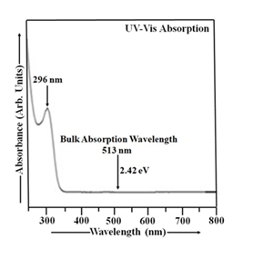
The absorbance spectrum, depicting the absorbance as a function of wavelength, is provided in Figure 1. The UV-Vis absorption spectrum of CdS nanoparticles exhibits a significant absorption peak in the ultraviolet wavelengths, while exhibiting minimal to no absorption in the near-infrared wavelengths. The CdS film's high transparency in the visible spectrum makes it a suitable window layer, allowing light to efficiently reach the absorber layer in optoelectronic devices [47]. The UV-Vis spectrum was collected over the 250-800 nm wavelength range. The CdS sample used in this study was prepared as a suspension of CdS nanoparticles in double distilled water, serving as the reference solution [1, 2]. The thioglycerol concentration in CdS sample was 1.904 M. This CdS sample exhibits a UV-Vis absorption peak at 296 nm, corresponding to an energy gap of approximately 4.19 eV. The particle size in this sample was found to be 4.60 nm. The optical absorption spectrum of CdS nanoparticles exhibits a blue shift compared to bulk CdS, which has a band gap of 2.42 eV and an absorption peak at 513 nm, due to quantum confinement effects [1-3].
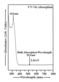
The absorbance curve for Mn-doped CdS nanoparticles, displaying its variation with wavelength, is shown in Figure 2. The analysis was performed across the UV-Vis spectral range, specifically from 250 to 800 nm. A suspension of CdS:Mn nanoparticles in double distilled water was used as the reference solution in this case [26]. The thioglycerol concentration in CdS:Mn sample was 1.904 M. The molarity of manganese chloride in this sample is 0.065 M. A prominent UV-Vis absorption peak, centered at 316 nm (energy gap ~ 3.93 eV), was detected in the Mn doped CdS sample. This peak signifies a significant absorption of ultraviolet and visible light by the material. The blue shift in the Mn-doped CdS nanoparticle absorption spectrum is a consequence of size quantization, causing a shift in energy levels due to the nanoscale dimensions of the material [26]. Based on the analysis, the particle size in CdS:Mn sample is estimated to be 4.79 nm. Analysis of Figure 1 and Figure 2 reveals a clear trend of increasing CdS:Mn nanoparticle size when thioglycerol concentration is held constant.
The larger size of CdS:Mn nanoparticles, as indicated by their UV-Vis absorption spectrum, is due to the quantum size effect and the influence of Mn doping on nanoparticle growth. Mn doping can alter the growth mechanism, leading to larger particle sizes compared to undoped CdS nanoparticles (Figure 1). Mn doping can alter the growth kinetics of CdS nanoparticles. For instance, manganese ions can act as nucleation sites or influence the rate of CdS growth, potentially leading to larger particles compared to undoped CdS. The band gap of CdS nanoparticles also increases with decreasing size. Mn doping further enhances this quantum size effect, leading to a larger band gap in CdS:Mn nanoparticles compared to undoped ones. The blue shift in the absorption edge of CdS:Mn nanoparticles, compared to undoped ones, is a clear indication that the size of the doped nanoparticles is larger. This blue shift suggests that the doped nanoparticles have a larger energy gap, indicating a larger average particle size, as shown in Figure 2. CdS:Mn nanoparticles offer several advantages over undoped CdS nanoparticles, particularly due to their larger particle size and enhanced photocatalytic activity. These advantages stem from the ability of Mn doping to alter the optical and structural properties of CdS, leading to improved performance in various applications like photocatalysis and solar cells. Mn doping can create new energy levels within the CdS bandgap, facilitating electron-hole separation and enhancing photocatalytic activity. Mn doping can improve the stability of CdS nanoparticles, making them more resistant to degradation under light exposure. The larger particle size and altered optical properties of Mn-doped CdS can lead to increased absorption of visible light, expanding the range of light that can be utilized for photocatalytic processes. Mn doping allows for the tuning of optical properties, such as the band gap and absorption spectra, which can be beneficial for specific applications, as shown in a study on CdS:Mn quantum dots in solar cells. Mn doping can improve the performance of CdS-based solar cells by increasing the efficiency of charge separation and transfer. The synthesis of Mn-doped CdS can lead to different morphologies (e.g, scale-like, needle-like) and particle sizes, which can be beneficial for specific applications, as discussed in a study on CdS:Mn thin films [1, 2, 26, 48-55]. Mn-doped CdS nanoparticles offer several advantages over undoped CdS nanoparticles, including enhanced stability, improved photoluminescence, and the potential for tunable optical properties. These improvements are particularly valuable in applications like solar cells, photocatalysis, and optoelectronic devices. Mn doping can increase the stability and resistance of CdS nanoparticles to photodegradation, leading to longer-lasting and more durable devices. Mn doping can alter the photoluminescence (PL) properties of CdS nanoparticles, potentially leading to changes in emission color and intensity. In some cases, Mn doping can even result in a dual-color emission, where the host CdS material emits blue light and the Mn dopant emits red light. Mn doping can modify the band gap of CdS nanoparticles, affecting their optical absorption and emission wavelengths. This tunability can be useful for designing devices that operate at specific wavelengths or have enhanced sensitivity to certain light sources. Mn doping can enhance the photocatalytic activity of CdS nanoparticles, making them more effective at breaking down pollutants and other substances under light irradiation. The combination of enhanced stability, improved PL, and tunable optical properties makes CdS:Mn nanoparticles attractive for a wide range of applications, including: Solar cells: Mn doping can improve the efficiency of CdS-based solar cells by enhancing light absorption and electron transfer. Photocatalysis: Mn doping can improve the photocatalytic activity of CdS nanoparticles, making them more effective at breaking down pollutants. Optoelectronic devices: Mn doping can lead to changes in the optical properties of CdS nanoparticles, which can be used to create new types of sensors, LEDs, and other optoelectronic devices. Bioimaging and drug delivery: The photoluminescence of CdS:Mn nanoparticles can be used for bioimaging and targeted drug delivery [1, 2, 19, 26, 34, 48, 49, 56-58].
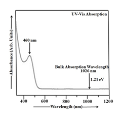
Figure 3 displays the absorbance spectrum of room-temperature Cu2S nanoparticles. The optical behavior of Cu2S nanoparticles was characterized through absorbance data spanning 370-1200 nm. The thioglycerol concentration in Cu2S sample is 0.952 M. UV-Vis absorption of Cu2S nanoparticles was measured with double distilled water as the reference [1, 8]. Figure 3 reveals an absorption peak at 460 nm, corresponding to an energy gap of approximately 2.70 eV, and thus occurring within the shorter wavelength region of the spectrum. Cu2S, with a narrow band gap of ~1.21 eV at room temperature, exhibits a shift in its absorption peak towards shorter wavelengths as the energy gap increases, as shown in Figure 3. The particle size measurement for Cu2S sample yielded a value of 8.59 nm.
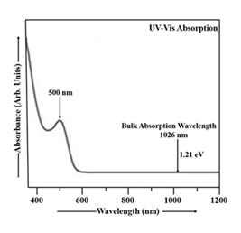
Employing UV-Vis absorption spectroscopy, the optical absorption characteristics of Mn-doped Cu2S nanoparticles were analyzed. The UV-Vis absorption data for the Mn-doped Cu2S nanoparticles, recorded across the 350-1200 nm range, are visualized in Figure 4. The thioglycerol concentration in Mn doped Cu2S sample is 0.952 M. The molarity of manganese chloride in this sample is 0.035 M. UV-Vis absorption spectroscopy was employed to study the Mn-doped Cu2S nanoparticles, using double distilled water as a reference [35]. The absorption peak at 500 nm in Mn-doped CdS indicates that the material strongly absorbs light at this wavelength, corresponding to an energy gap of approximately 2.48 eV. The bulk Cu2S material absorbs light at 1026 nm and has a band gap of 1.21 eV. When Mn is doped into Cu2S nanoparticles, the UV-Vis absorption spectrum shifts towards shorter wavelengths (blue shift) as the band gap increases from 1.21 eV to 2.48 eV. This blue shift is also accompanied by a decrease in the size of the Cu2S nanoparticles as the energy gap increases [35]. The particle size in Cu2S:Mn sample was found to be 10.07 nm.
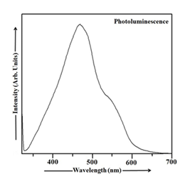
In UV-Vis absorption spectra, Mn doping leads to a red shift and broadening of the absorption band compared to undoped Cu2S, indicating larger particle sizes in Mn-doped nanoparticles. This is because doping alters the electronic structure and optical properties, leading to the formation of new energy levels and absorption bands within the band gap. Mn-doped Cu2S offers advantages in various applications like optoelectronic devices, photocatalysis, and spintronics, due to enhanced light absorption, improved charge transport, and potential for new functionalities. UV-Vis spectroscopy measures the absorption of light by a material at different wavelengths. The position and shape of absorption bands can provide information about the electronic structure and particle size of the material. Larger nanoparticles generally exhibit red-shifted and broader absorption bands compared to smaller ones. When Mn is doped into Cu2S, it introduces new electronic states within the band gap, which leads to new absorption bands at lower wavelengths (red shift) and broader absorption bands. This indicates an increase in the effective particle size. The red shift and broadening of the absorption bands mean that Mn-doped Cu2S nanoparticles can absorb light in a wider range of the visible spectrum. Mn doping can alter the electrical conductivity and charge transport properties of Cu2S, making it useful for applications like thermoelectric devices and solar cells. The introduction of Mn can lead to new functionalities, such as magnetism and luminescence, making Mn-doped Cu2S suitable for spintronics and optoelectronic applications. Mn-doped Cu2S can be used as a light absorber or active layer in solar cells, LEDs, and other optoelectronic devices. The enhanced light absorption and improved charge transport properties can make Mn-doped Cu2S a more efficient photocatalyst for reactions like water splitting or air purification. Mn's magnetic properties can be used to create new spin-dependent devices and functionalities in spintronic applications [1, 8, 35, 59-63]. The PL spectrum obtained from CdS nanoparticles at room temperature is visualized in Figure 5. Nanoparticles exhibited a significantly higher quantum luminescence efficiency than their bulk counterparts, as evidenced by the room temperature emission and excitation spectra [1, 64]. In the CdS sample, the light used to excite the material had wavelengths between 318 and 343 nm, and the emitted light had wavelengths ranging from 343 to 700 nm. The CdS particles were excited at 328 nm and the emission is located at 469 nm (energy gap 2.65 eV). From Figure 5, it is clearly observed that the PL spectrum of CdS nanoparticles exhibits a blue shift [1, 64], meaning the emission peak is observed at shorter wavelength compared to the bulk CdS material.
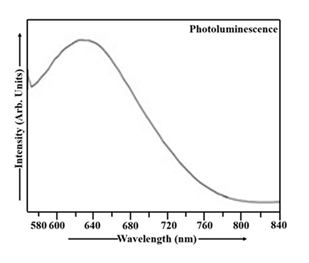
The PL spectrum of Mn-doped CdS nanoparticles measured at room temperature is depicted in Figure 6. The appropriate filters were used to record the PL spectrum of CdS:Mn sample from 560 to 626 nm in excitation mode and 626 to 840 nm in emission mode. The photoluminescence spectrum in Figure 6 reveals a peak at 631 nm (energy gap ~ 1.97 eV), characteristic of the Mn-doped CdS sample. The observed red shift [26] in the PL spectrum of the CdS:Mn sample is apparent in Figure 6.
CdS:Mn nanoparticles exhibit a red shift in their PL spectrum, while undoped CdS nanoparticles show a blue shift. This difference stems from the introduction of manganese ions into the CdS lattice, which alter the energy levels and transitions involved in PL emission. CdS:Mn nanoparticles offer enhanced performance in applications like photocatalysis and optoelectronics compared to their undoped counterparts. Mn²⁺ ions introduce new energy levels within the band gap of CdS, which can interact with the existing CdS energy levels. This interaction, particularly the splitting of Mn²⁺ energy levels, influences the energy of emitted photons and leads to a shift towards lower energy (red shift).
When CdS nanoparticles are excited, the energy can be transferred to the Mn²⁺ ions. The subsequent emission from Mn²⁺ ions results in a characteristic red emission. Doping with Mn can enhance the PL intensity and efficiency of CdS nanoparticles, making them suitable for various applications. In the case of undoped CdS nanoparticles, the quantum confinement effect, where the size of the nanoparticle plays a role in its electronic properties, can lead to a blue shift. Smaller nanoparticles have higher energy levels and emit photons at shorter wavelengths (blue region). Defect states within the CdS lattice can also contribute to emission, and these defects may have different energy levels compared to the ideal band gap, leading to shifts in the PL spectrum. CdS:Mn nanoparticles can exhibit improved photocatalytic activity, including better visible light absorption and charge separation compared to undoped CdS. Mn doping can lead to changes in the optical and electronic properties of CdS, making them suitable for applications like solar cells, LEDs, and photodetectors. The emission characteristics of Mn-doped CdS can be tailored by adjusting the Mn concentration, providing flexibility in their application. Mn doping can enhance the stability of CdS nanoparticles in various environments, making them more durable for long-term use [1, 2, 26, 35, 48, 52, 56, 65, 66].
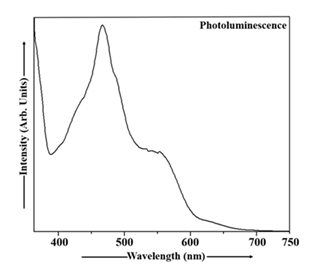
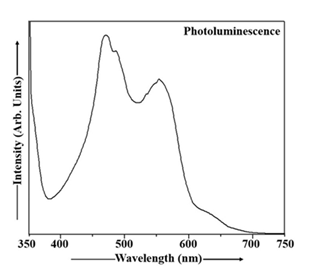
Figure 7 shows the photoluminescence characteristics of Cu2S nanoparticles measured under room temperature conditions. Photoluminescence spectra were collected across a range of 348 to 360 nm in the excitation domain and 360 to 750 nm in the emission domain. Spectral filtering was applied to isolate the desired emission wavelengths. In Cu2S sample, the excitation wavelength of 348 nm was used exciting the Cu2S particles and the maximum intensity of the emission peak was observed at 469 nm (energy gap 2.65 eV). The PL emission spectrum of Cu2S nanoparticles, displayed in Figure 7, exhibits a blue shift.The photoluminescence emission spectrum of Mn doped Cu2S nanoparticles, obtained at room temperature, is depicted in Figure 8. This PL spectrum was acquired with excitation ranging from 342 to 367 nm and emission spanning 367 to 750 nm, employing suitable optical filters. The Cu2S:Mn nanoparticles were excited at 352 nm and the PL peak was observed at 471 nm (energy gap ~ 2.63 eV). Analysis of the PL emission spectrum of Cu2S:Mn nanocrystals in Figure 8 reveals the presence of a blue shift.
Both undoped and Cu2S:Mn nanoparticles exhibit a blue shift in their PL spectra, but Mn doping offers advantages in applications. The blue shift in both cases is primarily due to quantum confinement effects caused by the small size of the nanoparticles. Mn doping introduces localized energy levels within the band gap of Cu2S, leading to a distinct emission peak from the Mn2+ ion. This allows for a tunable emission spectrum and enhanced PL intensity in Mn-doped samples, making them more versatile for applications like optoelectronics and photocatalysis. The blue shift in undoped Cu2S nanoparticles is a consequence of quantum confinement. As the size of the nanoparticles decreases, the energy levels of the electrons and holes become quantized, leading to an increase in the bandgap energy and a shift towards shorter wavelengths (blue) in the PL spectrum. While quantum confinement still plays a role, the presence of Mn2+ ions introduces localized energy levels within the Cu2S band gap. These Mn2+ levels can absorb light energy and emit light at specific wavelengths, contributing to the observed PL spectrum. The blue shift in this case can be attributed to a combination of the quantum confinement effect and the energy levels associated with the Mn dopant. Mn doping allows for control over the emission wavelength, as the PL spectrum is influenced by both the quantum confinement of Cu2S and the emission from the Mn2+ ions. The Mn2+ ions can act as efficient light emitters, leading to increased PL intensity in Mn-doped samples compared to undoped Cu2S The unique PL properties of Mn-doped Cu2S make them suitable for various applications, such as: Photocatalysis: The enhanced PL and tunable emission can improve the photocatalytic efficiency of Cu2S. Optoelectronics: The controllable emission spectrum allows for use in light-emitting devices and other optoelectronic applications. Biomedical Applications: The PL properties can be used for bioimaging and other biomedical applications. In summary, while both undoped and Cu2S:Mn nanoparticles exhibit a blue shift due to quantum confinement, Mn doping introduces localized energy levels that enhance PL intensity and enable a wider range of applications [1, 8, 35, 59, 60, 62, 63, 67].
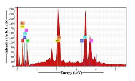
The sample's elemental composition was investigated using a combination of EDAX and elemental mapping techniques [1, 2]. The EDAX data for the dip-coated CdS thin film is presented in Figure 9. The atomic percentages of S, O, Pb, Cd, C, Pt, Sn, Na, and other elements in CdS sample, as determined by stoichiometric analysis, are summarized in Table 1. The presence of other elements like carbon, oxygen, and tin is a characteristic of the FTO glass substrate. Table 1 provides the data needed to calculate the Cd:S ratio in the dip-coated CdS thin film. For the CdS sample, the Cd:S ratio is 1.02, indicating a minor deviation from the stoichiometric value of 1. The Cd:S ratio exhibits a substantial increase as the dip time lengthens, resulting in a Cd-rich CdS phase and a thin film that is nearly ideally stoichiometric. The ratio of cadmium (Cd) to sulfur (S) in the CdS sample increases with a longer dip time. This means that for longer dip times, the CdS sample has more cadmium relative to sulfur.
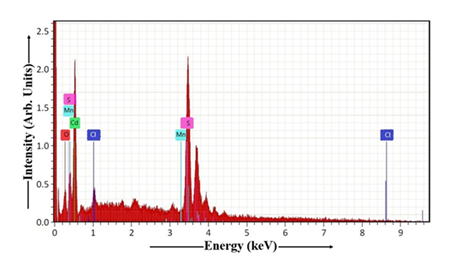
The EDAX spectrum, obtained from the Mn-doped CdS thin film deposited via dip coating, is visualized in Figure 10. Table 2 shows the stoichiometric atomic percentages of O, Cd, Cl, Mn, S, Na, C, and other elements in CdS:Mn sample. FTO glass substrate is composed of tin oxide, fluorine, and other elements like carbon and oxygen. For calculating the Cd:S ratio in the dip-coated CdS:Mn thin film, the data from Table 2 is essential. Analysis of the CdS:Mn sample reveals a cadmium to sulfur ratio of 1.00. The result demonstrates that the Cd and S atoms are present in a 1:1 ratio, resulting in a perfect stoichiometry within the CdS thin film.
Mn-doped CdS thin films offer several advantages over undoped CdS thin films in various applications, primarily due to the ability to tailor their properties by controlling the doping concentration and achieving perfect stoichiometry. This allows for precise modulation of electrical, optical, and structural characteristics, leading to improved performance in devices like solar cells and other optoelectronic applications. Mn doping can modify the electrical conductivity, band gap energy, and optical absorption of CdS, enabling optimization for specific applications. In solar cells, for example, Mn doping can improve charge transport and reduce recombination, leading to higher efficiency and power output. Mn-doped CdS can be used in various optoelectronic devices, including photodetectors, sensors, and LEDs, due to its tunable
optical and electronic properties. Achieving a perfect or near-perfect stoichiometry (the correct ratio of Cd and S atoms) is crucial for the material's performance. Mn doping can help maintain or restore stoichiometry, especially when dealing with non-stoichiometric conditions in the original CdS film. This ensures consistent and reliable performance of the material. By incorporating Mn, it can help to reduce the number of defects in the CdS lattice, improving its overall quality and stability. Mn doping can enhance the photocatalytic activity of CdS, making it more efficient at degrading pollutants in wastewater or other applications. Mn doping offers a precise way to manipulate the electrical, optical, and structural properties of CdS, allowing for optimization for specific applications. In solar cells, for example, Mn doping can significantly improve charge separation and transport, leading to higher efficiency compared to undoped CdS. By reducing defects and controlling stoichiometry, Mn doping can improve the overall performance and stability of CdS thin films in various applications. The tunable properties of Mn-doped CdS make it suitable for a wide range of optoelectronic devices and other applications [1, 2, 26, 49, 68-70].
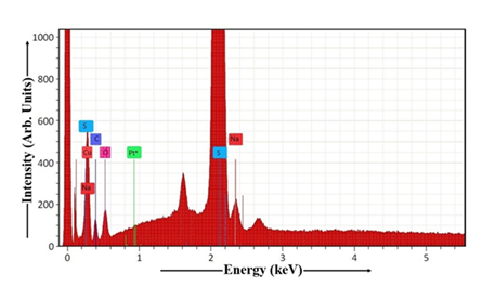
Figure 11 illustrates the EDAX analysis of the Cu2S thin film fabricated via the dip coating technique. Stoichiometric atomic percentages for the elements Cu, C, O, Na, Pt, S, and others present in Cu2S sample are presented in Table 3. FTO glass substrate contains carbon, and oxygen, as key components. Table 3 contains the information necessary to determine the Cu:S stoichiometry of the dip-coated Cu2S thin film. For the Mn-doped Cu2S sample, the molar ratio of cadmium to sulfur is 2.02. With longer dip times, the Cu:S ratio increases, indicating a Cu-rich Cu2S composition, suggesting the Cu2S thin film stoichiometry is close to the theoretical Cu2S composition.
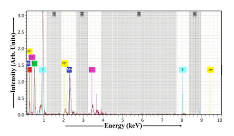
EDAX characterization of the dip-coated Mn-doped Cu2S thin film is shown in Figure 12. Table 4 contains the atomic percentage composition of Cu2S:Mn sample, including C, Cu, Mn, S, Cl, Pt, O, and other elements. FTO glass substrate is a transparent conductive oxide made of tin oxide (SnO2), fluorine (F), and possibly other elements like carbon and oxygen. FTO glass is as a transparent conductive oxide (TCO) substrate composed of fluorine-doped tin oxide (SnO2:F). This clarifies the material's composition and purpose as a conductive material that allows light to pass through. This transparent conductive oxide serves as a substrate, often used in optoelectronic devices like solar cells and displays. Using the data presented in Table 4, the Cu:S ratio of the dip-coated Cu2S:Mn thin film can be derived. The Mn-doped Cu2S sample's stoichiometry indicates a 2.00 Cu:S ratio. The analysis indicates that the Cu:S ratio is perfectly balanced, confirming a stoichiometric composition of the Cu2S:Mn thin film.
Mn-doped Cu2S thin films offer advantages over undoped Cu2S films, especially when perfect stoichiometry is crucial. Mn doping can enhance the thermoelectric properties of Cu2S by increasing the Se doping concentration limit. This improved Se doping helps to optimize the carrier concentration and adjust the electronic structure, leading to enhanced electrical conductivity and a lower lattice thermal conductivity. In essence, Mn doping fine-tunes the material's properties for improved performance in various applications. Mn doping can significantly increase the figure of merit (ZT) of Cu2S, a key indicator of thermoelectric performance. By increasing the Se doping concentration limit, Mn doping helps to optimize the material's electronic and thermal properties, leading to higher power generation efficiency. The increased Se doping due to Mn doping enhances the weighted mobility and electrical conductivity of Cu2S, making it a more efficient material for applications requiring electrical conductivity. Mn doping introduces lattice distortions and scatterers, which help to reduce the lattice thermal conductivity of Cu2S. This is beneficial in applications where high thermal conductivity can be detrimental, such as thermoelectric devices. Mn doping allows for a more precise control of the stoichiometry of Cu2S thin films, ensuring the material has the desired composition for specific applications. The improved thermoelectric and electrical properties of Mn-doped Cu2S make it a promising material for various applications, including thermoelectric generators, solar cells, and sensors. In summary, Mn doping provides a way to tailor the properties of Cu2S thin films for specific applications, particularly those where thermoelectric performance and precise stoichiometry are important. By increasing the Se doping concentration and improving the electronic and thermal properties, Mn doping makes Cu2S a more versatile and efficient material for various technologies [1, 8, 35, 71-75].
Mn-doped CdS and Cu2S nanoparticles and thin films are preferred over their undoped counterparts in many applications because doping with Mn enhances their optical and magnetic properties, leading to improved performance in areas like solar cells, luminescence, and magnetism. Specifically, Mn doping introduces magnetic moments, creating diluted magnetic semiconductors (DMS) with potential for enhanced magnetic and luminescent properties. Mn doping alters the electronic structure of CdS and Cu2S, leading to changes in their optical absorption and emission behavior. For example, in CdS, Mn doping introduces new luminescence peaks, potentially enhancing light emission. CdS:Mn nanoparticles exhibit ferromagnetism at room temperature, a feature not present in undoped CdS. This opens up possibilities for applications in spintronics and magnetic devices. Mn doping can increase the quantum efficiency of luminescence, meaning the nanoparticles emit more light for a given amount of excitation. The concentration of Mn dopant can be controlled, allowing for fine-tuning of the optical and magnetic properties of the resulting material. CdS:Mn nanoparticles have been explored as sensitizers in solar cells, leading to improved power conversion efficiency due to the increased absorption of light and enhanced electron transfer. In summary, Mn doping introduces desirable properties, including enhanced optical properties, ferromagnetism, and increased luminescence efficiency, making Mn-doped CdS and Cu2S nanoparticles and thin films more attractive for various applications compared to their undoped counterparts [1, 2, 8, 26, 35, 51, 54, 76].
|
Element |
At. No. |
Netto. |
Mass [%] |
Mass Norm [%] |
Atom [%] |
abs. error [%] (1 sigma) |
rel. error [%] (1 sigma |
|
Sulphur |
16 |
3737 |
6.11 |
4.46 |
31.61 |
1.03 |
16.95 |
|
Oxygen |
8 |
3622 |
6.06 |
4.43 |
13.09 |
1.03 |
17.06 |
|
Lead |
82 |
4169 |
7.65 |
5.60 |
3.36 |
0.32 |
4.15 |
|
Cadmium |
48 |
37576 |
76.19 |
55.72 |
32.34 |
2.59 |
3.40 |
|
Carbon |
6 |
8358 |
20.91 |
15.29 |
8.26 |
0.78 |
3.72 |
|
Platinum |
78 |
24058 |
0.00 |
0.00 |
0.00 |
0.00 |
1.78 |
|
Tin |
50 |
10979 |
15.75 |
11.52 |
4.03 |
0.64 |
4.10 |
|
Sodium |
11 |
4496 |
4.07 |
2.98 |
7.30 |
0.21 |
5.17 |
|
Sum |
136.74 |
100.00 |
100.00 |
Table 1: EDAX of CdS thin film.
|
Element |
At. No. |
Netto. |
Mass [%] |
Mass Norm [%] |
Atom [%] |
abs. error [%] (1 sigma) |
rel. error [%] (1 sigma |
|
Oxygen |
8 |
484 |
1.18 |
1.25 |
8.31 |
0.36 |
30.31 |
|
Cadmium |
48 |
5873 |
17.29 |
18.40 |
35.74 |
2.66 |
15.36 |
|
Chlorine |
17 |
365 |
0.98 |
1.04 |
2.81 |
0.12 |
12.25 |
|
Manganese |
25 |
2161 |
6.48 |
6.89 |
5.86 |
0.30 |
4.62 |
|
Sulphur |
16 |
16743 |
56.37 |
59.98 |
35.59 |
1.97 |
3.49 |
|
Sodium |
11 |
497 |
0.79 |
0.84 |
4.06 |
0.09 |
11.95 |
|
Carbon |
6 |
2567 |
10.90 |
11.60 |
7.63 |
0.48 |
4.36 |
|
Sum |
93.99 |
100.00 |
100.00 |
Table 2: EDAX of CdS:Mn thin film.
|
Element |
At. No. |
Netto. |
Mass [%] |
Mass Norm [%] |
Atom [%] |
abs. error [%] (1 sigma) |
rel. error [%] (1 sigma |
|
Copper |
29 |
24786 |
5.76 |
10.70 |
51.64 |
0.75 |
12.97 |
|
Carbon |
6 |
4849 |
1.75 |
3.25 |
11.47 |
0.30 |
17.17 |
|
Oxygen |
8 |
7768 |
1.56 |
2.91 |
8.51 |
0.25 |
16.14 |
|
Sodium |
11 |
8628 |
3.01 |
5.59 |
2.82 |
0.14 |
4.66 |
|
Platinum |
78 |
372461 |
0.00 |
0.00 |
0.00 |
0.00 |
1.78 |
|
Sulphur |
16 |
166173 |
41.74 |
77.55 |
25.56 |
1.58 |
3.80 |
|
Sum |
53.82 |
100.00 |
100.00 |
Table 3: EDAX of Cu2S thin film.
|
Element |
At. No. |
Netto. |
Mass [%] |
Mass Norm [%] |
Atom [%] |
abs. error [%] (1 sigma) |
rel. error [%] (1 sigma |
|
Carbon |
6 |
325 |
4.31 |
4.25 |
14.32 |
1.41 |
32.78 |
|
Copper |
29 |
2173 |
15.05 |
14.83 |
37.56 |
2.82 |
18.75 |
|
Manganese |
25 |
2160 |
7.58 |
7.47 |
11.44 |
0.37 |
4.83 |
|
Sulphur |
16 |
7090 |
51.75 |
51.00 |
18.78 |
7.66 |
14.80 |
|
Chlorine |
17 |
1352 |
12.43 |
12.25 |
9.18 |
0.61 |
4.88 |
|
Platinum |
78 |
562 |
0.00 |
0.00 |
0.00 |
0.00 |
1.78 |
|
Oxygen |
8 |
1423 |
10.34 |
10.20 |
8.72 |
0.53 |
5.12 |
|
Sum |
101.46 |
100.00 |
100.00 |
Table 4: EDAX of Cu2S:Mn thin film.
Conclusion
A room-temperature, non-aqueous chemical method was employed to synthesize Thioglycerol-capped CdS and Cu2S nanoparticles and Mn-doped DMS CdS and Cu2S nanoparticles. Thin films of CdS, Cu2S, Mn-doped CdS, and Cu2S thin films were prepared on FTO glass substrates by dip coating and then subjected to a 20-minute heat treatment at 420°C in air. Undoped and doped nanoparticles and thin films underwent comprehensive analysis using different techniques to assess their properties. This research explores the differences in experimental results between undoped and doped nanoparticles and thin films, showcasing the benefits of doped materials for various applications compared to their undoped versions.
Conflict of Interest
The authors declare no competing interests.
Source of funding
This research received no specific grant from any funding agency in the public, commercial, or not-for-profit sectors.
Data Availability Statement
The data that support the findings of this study are available within the article and its supplementary materials
References
- Darekar MS, Praveen BM. Synthesis and characterization of nanoparticles of semiconducting metal sulphide and their application. Physica Scripta 97 (2022): 065805.
- Darekar MS, Praveen B. M. Effects of heat treatment in air atmosphere on dip coating deposited CdS thin films for photo sensor applications. Journal of Modern Nanotechnology 3 (2023): 1-8.
- Saraf R. High efficiency and cost-effective Cu2S/CdS thin-film solar cell. Journal of Electrical and Electronics Engineering 2 (2012): 47-51.
- Li WZ, Liu Y, Wang ZY, et al. Fabrication of C and N co-doped CdS semiconductor photocatalysts derived from a novel Cd-MOF for enhancing photocatalytic performance. Journal of Environmental Chemical Engineering 12 (2024): 114204.
- Ismail W, Ibrahim G, Habib MA, et al. Advancement of physical and photoelectrochemical properties of nanostructured CdS thin films toward optoelectronic applications. Nanomaterials (Basel) 13 (2023): 1764.
- Billah A, Tojo F, Kubota S, et al. Organic molecule embedded CdS nanocomposite for hydrogen generation from water: Effect of precursors’ concentrations. International Journal of Hydrogen Energy 46 (2021): 35302-35310.
- Zavodinsky V, Gorkusha O, Kuz’menko A. Electronic structure of CdS nanoparticles and CdSe/CdS nanosystems. Semiconductor Science and Information Devices 4 (2022).
- Darekar MS, Praveen BM. High photosensitivity nanocrystalline p-Cu2S/n-FTO heterojunction photodetectors prepared by dip coating method. Journal of Modern Nanotechnology 3 (2023).
- Li X, Shen H, Li S, et al. Investigation on type-II Cu2S-CdS core/shell nanocrystals: synthesis and characterization. Journal of Materials Chemistry 20 (2009): 923-928.
- Patil M, Sharma D, Dive A, et al. Synthesis and characterization of Cu2S thin film deposited by chemical bath deposition method. Procedia Manufacturing 20 (2018): 505-508.
- Kumarakuru H, Coombes MJ, Neethling J H, et al. Fabrication of Cu2S nanoneedles by self-assembly of nanoparticles via simple wet chemical route. Journal of Alloys and Compounds 589 (2014): 67-75.
- Lv S, Suo H, Zhao X, et al. One-step synthesis of Cu2S nanostructures with two different morphologies on either side of a copper substrate. Journal of Alloys and Compounds 479 (2009): L43-L46.
- Zhang X, Pollitt S, Jung G, et al. Solution-processed Cu2S nanostructures for solar hydrogen production. Chemistry of Materials 35 (2023): 2371-2380.
- Chen CY, Jiang JR, Chuang WS, et al. Development of crystalline Cu2S nanowires via a direct synthesis process and its potential applications. Nanomaterials 10 (2020): 399.
- Farhadi S, Siadatnasab F. Copper(I) sulfide (Cu2S) nanoparticles from Cu(II) diethyldithiocarbamate: Synthesis, characterization and its application in ultrasound-assisted catalytic degradation of organic dye pollutants. Materials Research Bulletin 83 (2016): 345-353.
- Gurnani A, Inani H, Katharria YS, et al. Synthesis of cadmium sulfide (CdS) and copper(I) sulfide (Cu2S) nanoparticles for photovoltaic devices. International Conference on Functional Materials and Microwaves 8 (2015).
- Gowdhaman P, Praveen VN, Saravanan RSS, et al. Facile synthesis of undoped and Sn doped CdS nanoparticles for dye-sensitized solar cell applications. Optical Materials 120 (2021): 111465.
- Tiwary KP, Sharma K, Bala N, et al. Microwave assisted synthesis of undoped and Cu doped CdS nanoparticles and their structural, morphological and optical characterization. Materials Today: Proceedings 18 (2019): 1380-1387.
- Rashid MH, Koel A, Rang T, et al. Optical dynamics of copper-doped cadmium sulfide (CdS) and zinc sulfide (ZnS) quantum-dots core/shell nanoparticles. Nanomaterials 12 (2022): 2277.
- Tiwary KP, Ali F, Mishra RK, et al. Study of structural, morphological and optical properties of Cu and Ni doped CdS nanoparticles prepared by microwave assisted solvothermal method. Digest Journal of Nanomaterials and Biostructures 14 (2019): 305-313.
- Ghasempour A, Dehghan H, Ataee M, et al. Cadmium sulfide nanoparticles: Preparation, characterization, and biomedical applications. Molecules 28 (2023): 3857.
- Hadi IH, Khashan KS, Sulaiman D. Cadmium sulphide (CdS) nanoparticles: Preparation and characterization. Materials Today: Proceedings 42 (2021): 3054-3056.
- Gawande MB, Goswami A, Felpin FX, et al. Cu and Cu-based nanoparticles: Synthesis and applications in catalysis. Chemical Reviews 116 (2016): 3722-3811.
- Kumar M, Kumar C, Shukla S, et al. The size effect on the optical-electrical properties of Cu2S/CdS thin film towards the performance on Ag/p-Cu2S/n-CdS/ATO heterojunction diode. Materials Chemistry and Physics 297 (2023): 127305.
- Ghediya PR, Chaudhuri TK, Ray J, et al. Synthesis and characterizations of copper cadmium sulphide (CuCdS2) as potential absorber for thin film photovoltaics. Materials Chemistry and Physics 252 (2020): 123382.
- Darekar MS, Praveen BM. Hyperfine splitting and ferromagnetism in CdS:Mn nanoparticles for optoelectronic device applications. Journal of Semiconductors 44 (2023): 122502.
- -Rodriguez FJ, C.-Urbiola IR, H.-Landaverde MA, et al. Effects of incorporating manganese in CdS thin films elaborated by CBD and the performance of Schottky diodes TCO/CdS:Mn/C. Materials Chemistry and Physics 312 (2024): 128636.
- Azab AA, Ibrahim RS, Seoudi R. Investigating the effects of Mn content on the morphology and dielectric properties of CdS nanoparticles. Applied Physics A 130 (2024): 294.
- Mishra SK, Srivastava RK, Prakash SG, et al. Structural, optical and photoconductivity characteristics of manganese doped cadmium sulphide nanoparticles synthesized by co-precipitation method. Journal of Alloys and Compounds 513 (2012): 118-124.
- Orak C, Oguz T, Horoz S. Facile synthesis of Mn-doped CdS nanoparticles on carbon quantum dots: towards efficient photocatalysis. Journal of the Australian Ceramic Society 60 (2024): 1657-1667.
- Salimian S, Shayesteh SF. Luminescence properties of manganese doped CdS nanoparticles under various synthesis conditions. Acta Physica Polonica A 118 (2010): 633.
- Thangamuniyandi P, Nagaraj K, Velmurugan G, et al. Green synthesis of starch-capped CdS nanoparticles doped with copper(II) and manganese(II): Structural, optical, and photocatalytic properties. European Journal of Inorganic Chemistry 27 (2024).
- Fan L, Han J, Wei K, et al. Mn-doped CdS/Cu2O: An S-scheme heterojunction for photocatalytic hydrogen production. Journal of Alloys and Compounds 960 (2023): 170382.
- Verma MR, Shinde MD, Jagtap SS, et al. Synthesis and characterization of Mn doped CdS nanoparticles using chemical co-precipitation method. JETIR 6 (2019).
- Darekar MS, Praveen BM. Preparation of manganese doped copper sulphide nanoparticles by cost-favourable chemical method at room temperature. Journal of Metastable and Nanocrystalline Materials (2025).
- Haque Md M, Rahman A, Shahin Md S. I, et al. Manganese doped copper ferrite nanoparticles: A promising approach for organic dye elimination under light irradiation. Results in Chemistry 7 (2024): 101509.
- Tailor JP, Chaki SH, Deshpande MP. Comparative study between pure and manganese doped copper sulphide (CuS) nanoparticles. Nano Express 2 (2021): 010011.
- Saikia D, Saikia PK, Gogoi PK, et al. Synthesis, characterization and photovoltaic application of silver doped CdS/PVA nanocomposite thin films. Digest Journal of Nanomaterials and Biostructures 6 (2011): 589-597.
- Vasuki P, Radhika V, Mehala P. Characterization of manganese doped CdO thin films prepared by dip coating method. International Journal of Recent Scientific Research 15 (2024).
- Giri RK, Chaki SH, Khimani AJ, et al. Exploring the optoelectronic potential of dip coated CuInS2 thin films via morphological, structural, and photoresponse insights. Surfaces and Interfaces 61 (2025): 106098.
- Mukherjee A, Satpati B, Bhattacharyya SR, et al. Synthesis of nanocrystalline CdS thin film by SILAR and their characterization. Physica E: Low-dimensional Systems and Nanostructures 65 (2015): 51-55.
- Kim WY, Palve BM, Pathan HM, et al. Spray pyrolytic deposition of polycrystalline Cu2S thin films. Materials Chemistry and Physics 131 (2011): 525-528.
- Mahajan S, Kamble S, Lokhande R, et al. Opto-electrical properties studies of Cu2S thin film prepared by chemical bath deposition. International Journal of Creative Research Thoughts 11 (2023).
- Devi IR, Singh LR. Study of optical properties of CdS and Cu doped CdS thin films fabricated by chemical bath deposition technique. International Journal for Innovative Research in Multidisciplinary Field 6 (2020).
- Phasook N, Kamoldirok S, Yindeesuk W. Optical properties of Mn-doped CdS thin films grown by the SILAR method. Journal of Physics: Conference Series 1144 (2018): 012009.
- Gopi CVVM, Kim S-K. A strategy to improve the energy conversion efficiency and stability of quantum dot-sensitized solar cells using manganese-doped cadmium sulphide quantum dots. Dalton Transactions 44 (2015): 630.
- Okorie O, Buba A, Ramalan A. Optical and dielectric properties of cadmium sulphide thin film grown using chemical bath deposition technique. IOSR Journal of Applied Physics 9 (2017): 82-89.
- Ramya E, Kushavah D, Mohapatra J, et al. Ultrafast optical characteristics of Mn-doped CdS quantum dots. Results in Optics 13 (2023): 100560.
- Chauhan R, Kumar A, Chaudhary RP. Synthesis, structural and photocatalytic studies of Mn doped CdS nanoparticles. Research on Chemical Intermediates 39 (2012): 2.
- Ranjan R, Negi CMS, Choubey SK, et al. Study of structural, morphological and optical properties of Mn²⁺ doped CdS nanoparticles synthesized at various doping concentration. Chalcogenide Letters 20 (2023): 709-724.
- Ganguly A, Nath SS. Mn-doped CdS quantum dots as sensitizers in solar cells. Materials Science and Engineering B 255 (2020): 114532.
- Gupta AK, Kripal R. EPR and photoluminescence properties of Mn²⁺ doped CdS nanoparticles synthesized via co-precipitation method. Spectrochimica Acta Part A: Molecular and Biomolecular Spectroscopy 96 (2012): 626-631.
- Gadalla A, Almokhtar M, Abouelkhir AN. Effect of Mn doping on structural, optical and magnetic properties of CdS diluted magnetic semiconductor nanoparticles. Chalcogenide Letters 15 (2018): 207-218.
- Verma MR, Shinde MD, Jagtap SS, et al. Synthesis and characterization of Mn doped CdS nanoparticles using chemical co-precipitation method. JETIR 6 (2019).
- Patle US. Synthesis and characterization of Mn doped CdS nanoparticles prepared by chemical bath deposition method. International Journal of Science and Research (IJSR) 4 (2015).
- -Chory C, Remenyi C, Dem C, et al. Synthesis and characterization of manganese-doped CdS nanoparticles. Physical Chemistry Chemical Physics 5 (2003): 1639-1643.
- Patel NH, Deshpande MP, Bhatt SV, et al. Structural and magnetic properties of undoped and Mn doped CdS nanoparticles prepared by chemical co-precipitation method. Advanced Materials Letters 5 (2014): 671-677.
- Bodo B, Talukdar N, Kalita PK. Synthesis of CdS:Cu nanorods for application in photonic devices. International Journal of Engineering Research Applications (IJERA) 2 (2012): 1656-1659.
- Chen L, Hu H, Chen Y, et al. Plasmonic Cu2-xS nanoparticles: a brief introduction of optical properties and applications. Materials Advances 2 (2021): 907-926.
- Daskalakis I, Vamvasakis I, Papadas IT, et al. Surface defect engineering of mesoporous Cu/ZnS nanocrystal-linked networks for improved visible-light photocatalytic hydrogen production. Inorganic Chemistry Frontiers 7 (2020): 4687-4700.
- Daniel JE, Jesby CM, Plass KE, et al. Multinary tetrahedrite (Cu12-x-YMXNYSb4S13) nanoparticles: tailoring thermal and optical properties with copper-site dopants. Chemistry of Materials 36 (2024): 3246-3258.
- Cao S, Li C, Wang L, et al. Long-lived and well-resolved Mn²⁺ ion emissions in CuInS-ZnS quantum dots. Scientific Reports 4 (2014): 7510.
- Ming S-K, Taylor RA, O’Brien P, et al. Tunable, structural, morphological and optical properties of undoped, Mn, Ni and Ag doped CuInS2 thin films prepared by AACVD. Materials Science in Semiconductor Processing 137 (2021): 106224.
- Bangal M, Ashtaputre S, Marathe S, et al. Semiconducting nanoparticles. Hyperfine Interactions 160 (2005): 81-94.
- Sun D, Zhong H, Yao X, et al. A bright blue-shifted emission from Mn²⁺-doped CdS quantum dots. Materials Letters 125 (2014): 132-135.
- Khan MJI, Kanwal Z, Usmani MN. Shift in optical properties of Mn doped CdS (A DFT + U study). Materials Research Express 5 (2018): 015915.
- Chaki S, Tailor JP, Deshpande MP. Synthesis and characterizations of undoped and Mn doped CuS nanoparticles. Journal of Computational and Theoretical Nanoscience 20 (2014): 959-965.
- -Gomez J, DG.-Caballero A, RRosales K, et al. Influence of deposition temperature and fluorine doping on CdS properties: exploring applications in CdTe solar cells. Materials Science and Engineering B 309 (2024): 117646.
- Yilmaz S, Atasoy Y, Bacaksiz E, et al. Comparative studies of CdS, CdS:Al, CdS:Na and CdS:(Al-Na) thin films prepared by spray pyrolysis. Superlattices and Microstructures 88 (2015).
- Nalini, Deborrah SPM. Mn doped CdS thin films by using chemical bath deposition technique. Bodhi International Journal of Research in Humanities, Arts and Science 2 (2017): 174-181.
- Gong C, Zeng Z, Sun X, et al. Mn-doping method boosts Se doping concentration in Cu2S towards high thermoelectric performance. Journal of Materials Chemistry C 1 (2025).
- Zhuge F, Li X, Gan X, et al. Synthesis of stable amorphous Cu2S thin film by successive ion layer adsorption and reaction method. Materials Letters 63 (2008): 652-654.
- Liu GM, Schulmeyer T, Brotz J, et al. Interface properties and band alignment of Cu2S/CdS thin film solar cells. Thin Solid Films 431 (2003): 477-482.
- Pathan HM, Lokhande CD. Deposition of metal chalcogenide thin films by successive ionic layer adsorption and reaction (SILAR) method. Bulletin of Materials Science 27 (2004): 85-111.
- -German D, M.-Gil M, F.-Rios L, et al. Insights into the SILAR processing of CuxZn1-XS thin films via a chemical, structural, and optoelectronic assessment. ACS Omega 8 (2023).
- Dariani RS, Emami Z. Structural and optical studies of CdS and CdS:Ag nanoneedles prepared by a SILAR method. Ceramics International 41 (2015): 8820-8827.

 Impact Factor: * 2.9
 Acceptance Rate: 78.36%
  Time to first decision: 10.4 days
  Time from article received to acceptance: 2-3 weeks