Temperature Induced Microstructural Changes in InGaN/GaN Quantum Wells Observed by Electron Microscopy
Alexandra Gkanatsiou1*, Christos B Lioutas1, Ewa Grzanka2,3, Mike Leszczynski2,3
1Department of Physics, Aristotle University of Thessaloniki, GR-54124 Thessaloniki, Greece
2Institute of High Pressure Physics “Unipress”, Polish Academy of Sciences Sokolowska 29/37, 01-142 Warsaw, Poland
3TopGaN Ltd Sokolowska 29/37, 01-142 Warsaw, Poland
*Corresponding author: Alexandra Gkanatsiou, Department of Physics, Aristotle University of Thessaloniki, GR-54124 Thessaloniki, Greece.
Received : 09 February 2023; Accepted: 20 February 2023; Published: 03 March 2023
Article Information
Citation: Alexandra Gkanatsiou, Christos B Lioutas, Ewa Grzanka, Mike Leszczynski. Temperature Induced Microstructural Changes in Ingan/Gan Quantum Wells Observed by Electron Microscopy. Journal of Nanotechnology Research 5 (2023): 01-05.
DOI: 10.26502/jnr.2688-85210036
View / Download Pdf Share at FacebookAbstract
The present work concerns the microstructural characterization of multiple InGaN/GaN Quantum Well (QW) structures grown onto GaN on sapphire templates by Metalorganic Chemical Vapor Phase Epitaxy (MOVPE), using electron microscopy techniques (Transmission Electron Microscopy-TEM and Scanning Electron Microscopy-SEM). The TEM characterization showed V-shaped defects, including V-pits and trench defects on the surface of the as-grown sample. Post-growth annealing experiments were performed in order to determine whether a structural degradation of the structure has taken place. After annealing a very small density of V-defects was observed, having a beneficial impact on optoelectronics performance. The presence of sharp interfaces between the InGaN QWs and the GaN barriers gave us an indication of their good structural quality.
Keywords
<p>Transmission Electron Microscopy; Scanning Electron Microscopy; InGaN/GaN quantum wells; V-defects; Annealing</p>
Article Details
1. Introduction
InGaN is the key material in III-Nitride optoelectronic devices, such as light emitting diodes [1] (LEDs) and Laser Diodes (LDs) [2], operating in the blue and green ranges of the electromagnetic spectrum [3–5]. Single and multiple quantum wells (MQWs) based on GaN/InxGa1-xN serve as the active region in such devices, in which photons are generated by recombination of holes and electrons [6–9]. InGaN Quantum Wells (QWs) are typically grown on GaN substrates (bulk or templates grown on sapphire). However, it is difficult to grown high-quality InGaN on GaN, because it shows a large lattice mismatch to GaN (11%) [10]. Moreover, another issue dealing with is the low growth temperature needed for InGaN (700–800oC) [11], especially for high-In-content InGaN (where a further decrease in the growth temperature is required), as compared to the higher 950–1050oC for GaN growth [12]. These two factors induce a number of crystallographic defects, such as non-uniform indium distribution (indium concentration fluctuations) [13,14] and a large concentration of point defects. Such defects, in turn, deteriorate the optical properties of devices [6]. The most common defects present on the Metalorganic Chemical Vapor Phase Epitaxy (MOVPE) grown InGaN layer surfaces are V-pits and V-shaped trenches forming hexagonal loops [15]. These defects, contribute to the “green gap” problem [16-18], resulting in large polarization fields in the active region and thus reducing the radiative recombination rates [19,20]. Due to this problem, the external quantum efficiency (EQE) of green LEDs is significantly lower as compared to blue (the EQE of the blue LEDs exceeds 80%, whereas of the green LEDs is less than 60%) [21]. One of the “green gap” problem issues is the thermal instability of the QWs that takes place when higher temperatures are used for the overgrowth of the p-type layers on the QWs [22] (with the critical for thermal degradation temperature decreasing when increasing In content [23]). Thus, high In content InxGa1−xN layers tend to degrade when exposed to high temperatures (essential for good quality p-type layers [24,25]). Thus, the growth of blue and green emitters is challenging, requiring adjustments for the p-type layer quality and the thermal stability of the QW [19]. In this direction, great efforts are made by scientists [12,26] in order to grow high quality InGaN/GaN QWs that exhibit a low density of defects and a high uniformity of the interfaces. Thus, in this work, we report on the structural characterization of as-grown and annealed InGaN/GaN QWs grown onto GaN on sapphire templates by MOVPE, in order to study the quality of the structure. Transmission Electron Microscopy (TEM) and Scanning Electron Microscopy (SEM) experiments were performed.
2. Materials and methods
In this work, two MOVPE structures, labeled A and B respectively, were investigated. The MOVPE structures were deposited in an Aixtron close-coupled showerhead reactor of 3x2 in wafer configuration. As substrates, (0001) GaN on sapphire templates were used. Triethylgallium, trimethylindium, and ammonia were used as gallium, indium, and nitrogen precursors in MOVPE growth, respectively. Sample A, the as-grown sample, consists of two 10nm~In0.2Ga0.8N QWs/GaN barriers (Quantum Barrier-QB) capped with a 20 nm GaN layer (see Table I for the nominal thicknesses of the structure). This structure was grown on an Al0.05Ga0.95N layer, with nominal thickness 20nm and a nominally undoped buffer GaN layer. In order to determine whether degradation has taken place, we have performed post-growth annealing experiments at a temperature of 800oC (Sample B) in a protective atmosphere of ammonia and hydrogen for half an hour. All QWs/barriers were grown under identical growth conditions and contain the same in content (almost 18%).
|
QB – GaN – 20nm |
|
QW – InGaN – 10nm – 17.8% In |
|
QB – GaN – 10nm |
|
QW – InGaN – 10nm – 17.8% In |
|
QB – GaN – 10nm |
|
AlGaN – 20nm – 5% Al |
|
GaN – 1.5μm |
|
Sapphire |
Table 1: Sketch of the studied structure, showing the nominal thicknesses and elemental stoichiometric composition of the layers.
The structural quality of the as-grown and annealed samples was examined using a JEOL 2011 electron microscope operated at 200 kV. TEM/High Resolution TEM (HRTEM) observations were performed along the [ ] and [ ] zone axes of the structure. Cross-sectional TEM specimens were prepared by the wedge polishing technique [27], followed by argon ion-milling. SEM experiments were also performed in order to study the surface of the structure, using a Field-emission Scanning electron microscopy JEOL JSM-7610F Plus, supported by an Oxford AZtec Energy Advanced X-act energy dispersive X-ray spectroscopy (EDS) system.
3. Results and discussion
For both samples electron diffraction analysis reveals a strong epitaxial relationship between the epilayers and the sapphire substrate, besides the lattice mismatch at the interface plane. A typical electron diffraction pattern from an area containing the sapphire substrate as well as the first grown layers of Sample-A is shown in Figure 1.
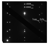
Plate 2: a) inoculated sheath blight Petri dish b) inoculated rice blast Petri dish.
Figure 1: A typical electron diffraction pattern obtained from a selected area containing part of the sapphire substrate and the first grown layers along [1120]. The very good epitaxial growth of GaN layer on the sapphire substrate is clear.
White arrows indicate the main reflections of the two phases (the Al2O3 reflections are denoted in italic). The c/a ratio is found equal to 1.62 ± 0.001 (for GaN), in good agreement with the referred in the literature value of 1.63 (ICDD PDF file 50–0792). The InN reflections are very weak, due to the small thickness of the layers. Moreover, they are very close to those of GaN and they are only detected far away from the central beam. For the structural characterization of the epilayers and interfaces, cross-sectional TEM samples were prepared. The conventional Bright Field (BF) TEM images of Fig. 2(a) and (b) show the entire multilayer structure of the as-grown (Sample-A) and annealed (Sample-B) samples, respectively; the layer thicknesses are in good agreement with the nominal ones (Table 1).
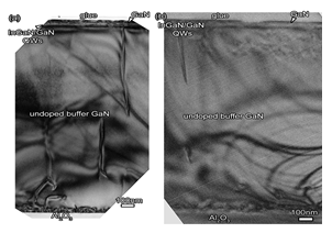
Figure 2: Bright Field TEM images showing the multilayer structure of (a) Sample-A (as-grown) and (b) Sample-B (annealed).
Some dislocations are observed in the undoped buffer layer (presenting a greater number in the as-grown sample case), but most of them do not reach the QWs and the structure surface. The TEM image of Fig. 3 (a) shows in a greater magnification the upper layers of the structure, revealing V-shaped defects of various sizes on the surface of Sample-A. Most of them (called V-pits), are connected to a threading dislocation, featuring a hexahedron pyramid morphology with six sidewalls on <1101> planes [28]. Their size does not exceed 60nm along [1100] and 20nm along [0001].
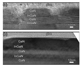
Figure 3: Bright Field TEM images showing a magnified part of the upper layers of (a) Sample-A (as-grown), (b) Sample-B (annealed).
According to Kim et al. [29], the V-pits creation is attributed to the strain in the high In mole fraction MQWs and also to the low surface mobility of adatoms on the InGaN layer. Apart from V-pits, trench-like defects of various sizes are also observed in the structure surface, which, according to Smalc-Koziorowska et al. [15], are formed due to the low temperature growth of the GaΝ QBs, where the basal stacking faults (BSFs) are created. Indeed, some BSFs are formed in the GaN layer, as shown in the HRTEM image of Figure 4.
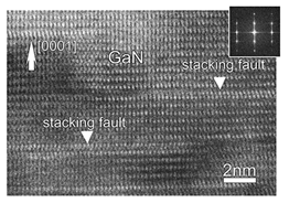
Figure 4: A HRTEM image showing the GaN layer, with some basal stacking faults noted with arrows (inset: FFT image of the area shown in Figure 4).
The Fast Fourier Transform (FFT) of the HRTEM image is presented as inset. The reconstruction of the lattice fringes via the inverse FFT (IFFT), using all spots of the FFT, was used in order to better indicate the stacking faults. In the IFFT image of Figure 5, a stacking fault is revealed in the magnified part of the image (with the stacking sequence noted), presented as inset.
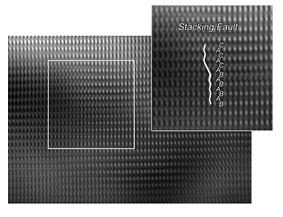
Figure 5: An IFFT image of the area showed in the HRTEM image of Fig. 4, where a stacking fault is indicated (inset: magnified part of a selected area of Figure 5).
Furthermore, the SEM experiments are consistent with the TEM observation results. Figure 6 shows the surface of Sample-A, where a V-pit and a trench defect are both indicated by arrows. The inset presents a magnified part of the SEM image (marked with a black colored rectangular shape), where a V-pit is highlighted.
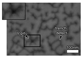
Figure 6: A typical SEM image obtained from the surface of Sample-A (as-grown), revealing the presence of V and trench defects (inset: magnified part showing a V-pit).
On the other hand, on the surface of Sample-B (annealed), an almost zero density of V-pits and trench defects is easy noticeable. Indeed, as shown in the low magnification TEM image of Figure 3 (b), the upper GaN layer is almost continuous. Moreover, the MQWs exhibit sharp interfaces with the GaN barriers. Thus, it is concluded that the presence of V-shaped defects is highly suppressed due to the 800oC annealing process. This fact is advantageous for optoelectronics, due to the fact that V-shaped defects result in their performance degradation (by increasing the probability of nonradiative recombination and by causing leakage current)[30]. On the other hand, some recent studies[21] have revealed that V-shaped defects can be beneficial for InGaN-based LEDs, but only when their size (greater than 100nm) and density are fully controlled. Finally, no structural degradation is evident in the QWs of the annealed Sample-B, in accordance with other studies[31].
4. Conclusions
In this work, InGaN/GaN QWs grown onto GaN on sapphire substrates are studied using electron microscopy techniques. The as-grown sample, features V-pits and trench defects of small size, which, according to other teams scientific work, deteriorate optoelectronics performance. After annealing at 800oC, a sharp surface with an almost zero density of V-shaped defects is observed, having a beneficial impact on optoelectronics. Thus, this fact, in combination with the homogeneous MQWs with sharp interfaces, shows the good growth of them.
Acknowledgments
This research is co-financed by Greece and the European Union (European Social Fund- ESF) through the Operational Programme «Human Resources Development, Education and Lifelong Learning» in the context of the project “Reinforcement of Postdoctoral Researchers - 2nd Cycle” (MIS-5033021), implemented by the State Scholarships Foundation (ΙΚΥ). It is also financed by project 2018/31/G/ ST5/03765 of the National Science Centre. This article has benefited from the contributions of the following people: Mrs. Catherine Breza (Centre for Research and Technology Hellas–CERTH) assisted, with particular interest, in the TEM observations and Professor Eleni Pavlidou plus Mrs. Chrysanthi Papoulia (Department of Physics, Aristotle University of Thessaloniki-AUTh) in the SEM observations.
Conflict of interest
The authors declared that they have no conflicts of interest to this work.
References
- S Nakamura, M Senoh, N Iwasa, et al. High-brightness InGaN blue, green and yellow light-emitting diodes with quantum well structures, Jpn. J Appl Phys 34 (1995): L797-L799.
- S Nakamura, M Senoh, S ichi Nagahama, et al. InGaN-based multi-quantum-well-structure laser diodes, Japanese. J Appl Physics Part 2 Lett 35 (1996).
- MD McCluskey, LT Romano, BS Krusor, et al. Interdiffusion of in and Ga in InGaN quantum wells. Appl Phys Lett 73 (1998): 1281-1283.
- S Nakamura, M Senoh, N Iwasa, et al. High?power InGaN single?quantum?well?structure blue and violet light?emitting diodes. Appl Phys Lett 67 (1995): 1868-1870.
- GP Dimitrakopulos, IG Vasileiadis, C Bazioti, et al. Compositional and strain analysis of In(Ga)N/GaN short period superlattices. J Appl Phys 123 (2018): 024304.
- M Sarzy?ski, E Grzanka, S Grzanka, et al. Indium incorporation into InGaN quantum wells grown on GaN narrow stripes, Materials (Basel) 12 (2019): 1-15.
- CC Chuo, CM Lee, JI Chyi. Interdiffusion of in and Ga in InGaN/GaN multiple quantum wells. Appl Phys Lett 78 (2001): 314-316.
- S Nakamura, M Senoh, S Nagahama, et al. Room?temperature continuous?wave operation of InGaN multi?quantum?well structure laser diodes. Appl Phys Lett 69 (1996): 4056-4058.
- B Van Daele, G Van Tendeloo, K Jacobs, et al. Formation of metallic In in InGaN?GaN multiquantum wells, Appl Phys Lett 85 (2004): 4379.
- M Leszczynski, H Teisseyre, T Suski, et al. Lattice parameters of gallium nitride. Appl Phys Lett 69 (1996): 73-75.
- M Grabowski, E Grzanka, S Grzanka, et al. The impact of point defects in n-type GaN layers on thermal decomposition of InGaN/GaN QWs. Sci Rep 11 (2021): 1-11.
- Y Wang, F Liang, D Zhao, et al. Effect of High Temperature Treatment on the Photoluminescence of InGaN Multiple Quantum Wells (2022).
- S Nakamura. The roles of structural imperfections in InGaN-based blue light- emitting diodes and laser diodes, Science (80-.). 281 (1998): 956-961.
- PP Micha?owski, E Grzanka, S Grzanka, et al. Indium concentration fluctuations in InGaN/GaN quantum wells. J Anal At Spectrom 34 (2019): 1718-1723.
- J Smalc-Koziorowska, E Grzanka, R Czernecki, et al. Elimination of trench defects and V-pits from InGaN/GaN structures. Appl Phys Lett 106 (2015).
- S Pleasants. Overcoming the “green gap,” Nat. Photonics. 7 (2013): 585-585.
- NK Van Der Laak, RA Oliver, MJ Kappers, et al. Role of gross well-width fluctuations in bright, green-emitting single InGaNGaN quantum well structures. Appl Phys Lett 90 (2007).
- H Jeong, HJ Jeong, HM Oh, et al. Carrier localization in In-rich InGaN/GaN multiple quantum wells for green light-emitting diodes. Sci Rep 5 (2015).
- A Lachowski, E Grzanka, S Grzanka, et al. Improving thermal stability of InGaN quantum wells by doping of GaN barrier layers. J Alloys Compd 900 (2022).
- IG Vasileiadis, L Lymperakis, A Adikimenakis, et al. Substitutional synthesis of sub-nanometer InGaN/GaN quantum wells with high indium content. Sci Rep 11 (2021): 1-13.
- S Zhou, X Liu, H Yan, et al. The effect of nanometre-scale V-pits on electronic and optical properties and efficiency droop of GaN-based green light-emitting diodes. Sci Rep 8 (2018).
- Z Li, J Liu, M Feng, et al. Suppression of thermal degradation of InGaN/GaN quantum wells in green laser diode structures during the epitaxial growth, Appl Phys Lett 103 (2013).
- MT Hardy, F Wu, P Shan Hsu, et al. True green semipolar InGaN-based laser diodes beyond critical thickness limits using limited area epitaxy. J Appl Phys 114 (2013): 183101.
- LT Romano, MD McCluskey, CG Van de Walle, et al. Phase separation in InGaN multiple quantum wells annealed at high nitrogen pressures. Appl Phys Lett 75 (1999): 3950-3952.
- V Hoffmann, A Mogilatenko, U Zeimer, et al. In-situ observation of InGaN quantum well decomposition during growth of laser diodes. Cryst Res Technol 50 (2015): 499-503.
- F Massabuau, M Kappers, C Humphreys, et al. Mechanisms preventing trench defect formation in InGaN/GaN quantum well structures using hydrogen during GaN barrier growth, Phys. Status Solidi Basic Res 254 (2017).
- J Chen, DG Ivey. Preparation of metallized GaN/sapphire cross sections for TEM analysis using wedge polishing. Micron 33 (2002): 489-492.
- A Hangleiter, F Hitzel, C Netzel, et al. Suppression of nonradiative recombination by V-shaped pits in GaInN/GaN quantum wells produces a large increase in the light emission efficiency. Phys Rev Lett 95 (2005).
- IH Kim, HS Park, YJ Park, et al. Formation of V-shaped pits in InGaN/GaN multiquantum wells and bulk InGaN films. Appl Phys Lett 73 (1998): 1634-1636.
- SW Chen, CJ Chang, TC Lu. Effect of strains and v-shaped pit structures on the performance of gan-based light-emitting diodes. Crystals 10 (2020).
- J Smalc-Koziorowska, E Grzanka, A Lachowski, et al. Role of Metal Vacancies in the Mechanism of Thermal Degradation of InGaN Quantum Wells. ACS Appl Mater Interfaces 13 (2021): 7476-7484.

 Impact Factor: * 2.9
 Acceptance Rate: 78.36%
  Time to first decision: 10.4 days
  Time from article received to acceptance: 2-3 weeks