Nanopillar-Based Light Emitting Diodes
Sonam Saxena, Hai-Feng Ji*
Department of Chemistry, Drexel University, Philadelphia, Pennsylvania, USA
*Corresponding Author: Hai-Feng Ji, Department of Chemistry, Drexel University, Philadelphia, PA 19104, Pennsylvania, USA
Received: 21 June 2019; Accepted: 08 July 2019; Published: 24 July 2019
Article Information
Citation:
Sonam Saxena and Hai-Feng Ji. Nanopillar-Based Light Emitting Diodes. Journal of Nanotechnology Research 2 (2019): 036-042.
DOI: 10.26502/jnr.2688-8521003
View / Download Pdf Share at FacebookAbstract
Daily life is surrounded by the use of optoelectronics in order to provide illumination for the most basic of routines. For this reason, research into the performance enhancement of such optoelectronic devices is paramount in order to understand methods of improving efficiency and thus conserving energy and resources. This review briefly summarized various techniques to fabricate nanopillars for enhancing performance of light emitting diode (LED), using etching masks, nanosphere lithography, integration of other materials, and MOVPE manipulation.
Keywords
<p>Nanopillar, Micropillar, Nanoparticle, LED</p>
Article Details
1. Introduction
The omnipresence of optoelectronics in daily life makes research into improving the device efficiency and performance very important. Optoelectronics include essentially any device that works to produce light, for example in military, medical, or commercial application. Common types of optoelectronic devices include photodiodes, solar cells, light emitting diodes (LEDs), optical fibers, and more. Planar LEDs are traditionally comprised of at least 3 functional layers, namely a p-doped layer, an active layer, and n-doped layer, as well as additional wells, barriers, and layers to the active region [1]. This layered structure allows the LED structures to be manipulated into whatever shape is desired, for example pillars or hexagonal or pyramidal with whatever base width and height is decided.
2. Processing Methods to Enhance Performance
In order to improve upon device performance, many methods have been conducted and most of them include etching and lithography. These methods work to manipulate the nanopillar layers of the device in order to reduce defects and increase photon ejection. Semiconductor etching can take form in a variety of ways, a popular one being inductively coupled plasma (ICP) etching. Nanosphere lithography is another method that fabricates homogenous nanoparticle arrays with pillars of different sizes, combining both top-down and bottom-up approaches by including both dots/structured layers as well as self-organization of particles in the lattice [2]. Fadil et al. attempted to solve the major obstacle of low quantum efficiency green-GaN based LEDs by nanopatterning the surface via nanosphere lithography [3]. The active region was etched, and improvement in the quantum efficiency resulted via lattice strain relaxation. Strain was introduced via the quantum-confined Stark effect (QCSE), which causes strong polarization within the quantum wells. Zhan-Xu et al. also fabricated periodic nanopillar arrays via the nanosphere lithography and optimized the diameter of each nanopillar [4]. The greatest enhancement that resulted was by a multiplier of 1.41 mA at an injection current of 20 mA, due to the bilayer film layered on substrate. Such results demonstrate the potential of integrating treatment and manipulation methods for greater performance of LED.
Similarly, other methods can be included into nanopillar and device formation as well. Thermal etching is a process that utilizes high temperatures to reveal specific grooves at interface boundaries between materials. Another method by Yakimov et al. tested the inclusion of low energy electron beam irradiation (LEEBI) on planar and nanopillar LED structures in order to enhance emissions from the device [5]. Their results demonstrated a blue shift of emission (from 2.92 eV to 2.98 ev) along with an increase in intensity from InGaN/GaN multiple quantum wells (MQWs) due to excitation of the lower n-GaN layer through the fabricated holes as well as decrease of strain and piezoelectric field in the quantum wells. This allows for redistribution of the electron beam irradiation, encouraging higher device performance. Sidewall passivation is another method seeking device enhancement. Choi et al. discovered the effects of KOH treatment, and sulfur passivation on MQWs of InGaN/GaN LEDs [6]. These methods were tested in attempt to reduce nanopillar damage, which works to enhance device performance. Results showed the following: nanopillars etched under specific optimal conditions demonstrated higher photoluminescent intensity, passivated nanopillars demonstrated reduced leakage current as well as increased electroluminescence, and sulfur passivation was stable but examined more using transmission electron microscopy.
3. Inclusion of other Materials to Enhance Performance
The use of nitride-based semiconductors seems traditional and effective, to some degree. But, many methods have been assessing the inclusion of different materials integrated into the nitride device to optimize device performance. Often this is via the inclusion of nanoparticles into the nanopillar diode array. For example, Ou et al. examined the inclusion of SiO2 and Au nanoparticles [7]. Often, planar reference LEDs suffer from significant QCSE, reducing the light extraction efficiency (LEE). The fabrication of this LED deposited a layer of SiO2 atop the planar surface and then used rapid thermal processing to form Au nanoparticles in the film laid. From here the nanopillar array was transferred using these particles and forming pillar heights of 580 nm. They demonstrated considerable enhancement by a factor of 4.08 and a blue shift in photoluminescent emissions, most likely due to the quantum well relaxation. This allows for greater scattering of photons as well as increased escaping of the light as the hindering piezoelectric field is released and the overlap of electrons and holes is enhanced [8]. In addition, the blue shift of emission peak signifies a shift to shorter wavelength and greater strain relaxation.
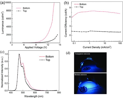
Another method by Guo et al. tested the inclusion of molybdenum disulfide in the plastic substrates of inverted organic LEDs (IOLEDs) in order to improve the original challenges of poor electron injection and instability [9]. They demonstrated a high quantum efficiency of 7.3% at a luminescence of 9141 cd m-2, which is a significantly improved value (see Figure 1). In addition, the MoS2-based LED developed a 1.8-fold increase in power efficiency, a significant luminescence increase from 100 to 5000 cd m-2, and stability in the maintenance of high brightness for 500 cycles. These results may be due to the decreased Fermi level, allowing for greater electron injection, as well as increased dipole-dipole interactions at the surface interface allowing for greater current density.

Figure 1: (a) Plot of luminescence vs applied voltage; (b) plot of current efficiency vs current density measured from top and bottom surfaces of Device E; (c) plot of normalized electroluminescence spectra measured from the top and bottom surfaces of device E; (d) photographs of the top and bottom surfaces in the upper and lower sections, respectively, measured at the same voltage. Reproduced with permission from [9]. Copyright 2017, RSC.
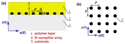
Silicon is also another element often included in the devices in an attempt to increase performance due to its ability to enhance near-field enhancement and better photon emission, thus improving light extraction. Ding et al. included silicon in white LEDs in an attempt to improve light conversion and efficiency [10]. They studied the guided mode from the array of Si nanoparticles integrated into the silica substrate of the device and covered by polymer layer. The Si nanopillar array allowed incoming light to couple to the guided modes in the polymer layer when the wave vectors were matched, causing improved scattering and electric field enhancement (see Figure 2).
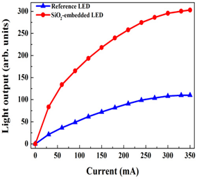
Another group to test the integration of silicon via nanopillars in LEDs is Jeon et al. This group tested the inclusion of SiO2 nanopillars embedded within the GaN template of the InGaN/GaN LED [11]. Here, undoped GaN films were grown using sapphire substrates via metal organic chemical vapor deposition (MOCVD) with a 100-nm thick SiO2 nanopillar layer deposited on top. A 10-nm thick Ni layer was placed in the SiO2 interlayer using e-beam evaporation. After undergoing ICP etching and removing the Ni to leave the pillars, SiO2 nanoparticles were embedded between and the undoped GaN region with quantum wells was regrown. After examining the SEM images, selective lateral overgrowth was seen due to the embedded SiO2 nanoparticles, causing air voids to form between nanopillars. The increased density by SiO2 nanoparticles with the air voids can contribute to enhanced (300%) photoluminescent (PL) intensity compared to the reference as well as enhanced light output, as seen in Figure 3. In addition, the strain relaxation by the nanopillars also contributes to providing a blue shift in PL (441 to 447 nm) and increase in intensity due to stronger overlap of electron and hole waveforms in the quantum wells.

Figure 2: (a) Diagram of the experimental layering, with the Si nanopillar array deposited atop silica substrate and a polymer layer laid atop; (b) Schematic of square Si nanopillar array. Reproduced with permission from [10]. Copyright 2015, OSA.

Figure 3: Plot of the current curves for reference (planar) LED versus the current curve for the LED with embedded SiO2 nanoparticles. The SiO2 LED demonstrates higher light output at almost all the current values tested. Reproduced with permission from [11]. Copyright 2014, OSA.
Another group, Wei et al., tested the inclusion of CsCl nanoislands in III-nitride wide bandgap LEDs in order to study the improvement of photon ejection and light scattering [12]. The new method uses roughening of the surface of the LED using integrated CsCl nanoislands as an etch mask for hemispherical nanostructures. Results displayed this technique as a low-cost and effective alternative to increase extraction efficiency by about 70% at 350 mA injection current. In addition, increasing the size of the CsCl nanoislands elevated results even more, by increasing extraction efficiency to as much as 77.9% for a 650 nm island. Finally, the roughened LED red shift displayed the decrease of compressive strain in the quantum wells, also leading to improved performance.
4. Various Types of LEDs
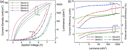
In addition, some groups researched the use of various types of LEDs, rather than the type of material added. Ryu et al. tested the functioning of AlGaInP-based LEDs with vertical injection geometry with n-AlGaInP nanopillars etched as well. These LEDs provided up to 25% power enhancement due to the reduction of internal reflection/refractive index between materials, which allows a greater critical angle for photons to escape through [13]. Similarly, Guo et al. examined the use of inverted organic LEDs (IOLEDs) on plastic substrates, and tested the inclusion of molybdenum disulfide (MoS2) with four experimental devices [14]. Devices A and B were tested without the inclusion of MoS2, and devices C and D were tested with the inclusion of MoS2. Performances of the devices are seen in Figure 4. Results show that the MoS2 treated IOLEDs can achieve higher quantum efficiency as well as improved power efficiency (compared respectively to flexible blue and glass-based reference IOLEDs). One explanation for the improved performance is the increased van der Waals bonding and resulting formation of MoS2 nanopillar arrays, enabling better light extraction. The treated IOLEDs not only show increased quantum and power efficiencies, but also enhanced current efficiency as well as mechanical stability as the luminescence persevered even after many bending cycles.

Figures 4: (a) Shows curves of current density and luminescence of the various devices, A and B not treated with MoS2, C and D treated with MoS2. Devices C and D show higher values than A and B for both; (b) Shows curves of current efficiency and external quantum efficiency. Devices C and D show higher values than A and B for both. Reproduced with permission from [14]. Copyright 2017, RSC.
5. Variation of Fabrication Processes
Another way to improve LED performance is to optimize the fabrication processes of the devices. Many research groups used methods of metal-organic vapor phase epitaxy (MOVPE), also known as metal organic chemical vapor deposition (MOCVD), to create the LED structures. MOVPE is a growth technique where molecular gases interact on a heated substrate base in order to produce a semiconductor layer on top, producing a direct band gap. The experimental device was able to operate as an LED under the condition that the diameter of the nanopillars was about 1000 nm with a separation distance of less than 1000 nm between pillars [15]. These optimal conditions demonstrated emittance of high energy blue light, showing promising results for future work. In addition, another group attempted the fabrication of blue GaN-based LEDs with coating procedures to form white LEDs. The process used MOCVD to grow GaN layers on sapphire substrates on the device. From here, a series of techniques were used for the microfabrication, including mesa etching, metal deposition, lift-off, and annealing [16]. Resulting intensity measurements for the blue LEDs was as high as 80 mcd. Coating procedures included the use of phosphor epoxy solution atop the blue chips, producing white LED lamps. This resulting intensity of the white LEDs was as high as 40 lm W-1 at 20 mA current. These efforts demonstrate MOVPE/MOCVD as an effective fabrication process for the enhancement of LED devices.
6. Conclusion
The study of increasing efficiency of LED performance is paramount due to the wide range of pervasive applications that such devices have in daily life. Numerous studies have shown ways to improve performance, but comparisons among them will demonstrate which is the best for the commercial use and energy conservation. Some work by releasing quantum well strain and QCSE, some aim to increase interactions between layers in order to promote electron ejection, and many use a combination of various techniques. Among the most successful seem to be the inclusion of nanoparticles and the use of ICP etching and LEEBI. Future work will require more in-depth studies and a range of numerical comparisons between results.
References
- Colson P, Henrist C, Cloots R. Nanosphere Lithography: A Powerful Method for the Controlled Manufacturing of Nanomaterials. Journal of Nanomaterials (2013).
- Fadil A, Ou Y, Zhan T, et al. Fabrication and improvement of nanopillar InGaN/GaN light-emitting diodes using nanosphere lithography. Journal of Nanophotonics 9 (2015).
- Zhan-Xu C, Yuan R, Guo-Hui X, et al. Enhancing light extraction of GaN-based blue light-emitting diodes by a tuned nanopillar array. Chinese Physics B 23 (2014).
- Yakimov E, Vergeles P. Low energy electron beam irradiation effect on optical properties of nanopillar MQW InGaN/GaN structures. AIP Conference Proceedings 1563 (2015): 268.
- Yakimov E, Vergeles P. Microcathodoluminescence spectra evolution for planar and nanopillar multiquantum-well GaN-based structures as a function of electron irradiation dose. Journal of vacuum science and technology B 32 (2013).
- Choi W, You G, Abraham M, et al. Sidewall passivation for InGaN/GaN nanopillar light emitting diodes. Journal of Applied Physics 116 (2014).
- Ou Y, Ahmed F, Haiyan O. Fabrication of InGaN/GaN nanopillar light-emitting diode arrays. 3rd European-Asian workshop on Light-Emitting Diodes (2015).
- Ou Y, Iida D, Liu J, et al. Efficiency enhancement of InGaN amber MQWs using nanopillar structures. Nanophotonics 7 (2018): 317-322.
- Guo K, Si C, Han C, et al. High-Performance Flexible Inverted Organic Light-Emitting Diodes by Exploiting MoS2 Nanopillar Arrays as Electron-injecting and Light-coupling Layer. Nanoscale 9 (2017).
- Ding P, Li M, He J, et al. Guided mode caused by silicon nanopillar array for light emission enhancement in color-converting LED. Optics Express 23 (2015): 21477-21489.
- Jeon D, Jang L, Cho H, et al. Enhanced optical output performance in InGaN/GaN light-emitting diode embedded with SiO2 nanoparticles. Optics Express 22 (2014): 21454-21459.
- Wei T, Kong Q, Wang J, et al. Improving light extraction of InGaN-based light emitting diodes with a roughened p-GaN surface using CsCl nano-islands. Optics Express 19 (2011): 1065-1071.
- Ryu H, Park M, Oh S, et al. Vertical-Injection AlGaInP LEDs with n-AlGaInP Nanopillars Fabricated by Self-Assembled ITO-Based Nanodots. Nanoscale Research Letters 10 (2015): 356.
- Guo K, Si C, Han C, et al. High-Performance Flexible Inverted Organic Light-Emitting Diodes by Exploiting MoS2 Nanopillar Arrays as Electron-injecting and Light-coupling Layer. Nanoscale 9 (2017).
- Albert S, Bengoechea-Encabo A, Ledig J, et al. Demonstration of (In, Ga)N/GaN Core–Shell Micro Light-Emitting Diodes Grown by Molecular Beam Epitaxy on Ordered MOVPE GaN Pillars. Crystal Growth and Design 15 (2015): 3661-3665.
- Nguyen X, Nguyen T, Chau V, et al. The fabrication of GaN-based light emitting diodes (LEDs). Advances in Natural Sciences: Nanoscience and Nanotechnology 1 (2010).

 Impact Factor: * 2.9
 Acceptance Rate: 78.36%
  Time to first decision: 10.4 days
  Time from article received to acceptance: 2-3 weeks